JBOT – An Easy QRP linear amplifier
JBOT stands for Just a Bunch of Transistors. It is a simple, stable and easy to build 5 watts linear amplifier build out of a bunch of ordinary low power NPN transistors.
Why another linear amp?
For many of us, getting hold of high power RF transistors is impossible. They are also expensive and easily blown. In the last decade, hams have pressed the power MoSFETs into use as RF devices. This has been a mixed success. The power FETs (mostly the IRF series for International Rectifiers) have very high input and output capacitance, they need higher drain voltage and they are very non-linear devices. As result, IRF device based RF power amplifiers have remained beyond easy replication for the average homebrewer.
Often, the RF power amplifiers are run flat-out without any attempt at stabilizing the performance, This has to lead to a lot of grief.
The BITX’s linear amplifier painfully illustrates both these issues. The IRF510 takes a lot to get it going. Many of those who scratch build it on their own often found themselves struggling with stability and insufficient power output.
The inspiration from this power amplifier came from watching a colleague assemble an incredibly fast computer by adding together a number of ordinary hard disks and old mother boards. By stringing them all together, he was able to extract an amazing performance. When I asked him what kind of architecture this was, his reply was “It is JBOD (Just a bunch of disks)”.
Paralleling transistors is not new to hams. I can recall an article by Doug (sk W1FB) in a 1970s QST where he had paralleled up six 2N3904s to generate a single watt of power. Harry’s small linear amplifier pumped up to 23dBm out of general purpose NPN transistors.
In this design, the attempt is to apply these principles to higher power output from the 2N2218 variety of transistors to get 5 watts of clean, stable and linear output from a 1milliwatt signal.
What is JBOT?
JBOT stands for Just a Bunch of Transistors. This linear replaces one big RF power device with a bunch of smaller, ordinary transistors.
- Each transistor handles less power, simple clip-on heat sinks are enough.
- Each output transistor has its own emitter degeneration, making the configuration very stable.
- Any general purpose NPN transistor rated for more than 500 mA current with metal can will work.
- The drivers are biased for higher than usual current to prevent saturation and good linearity.
Circuit Design
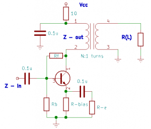
The circuit is a quite simple and straight forward three stage amplifier.
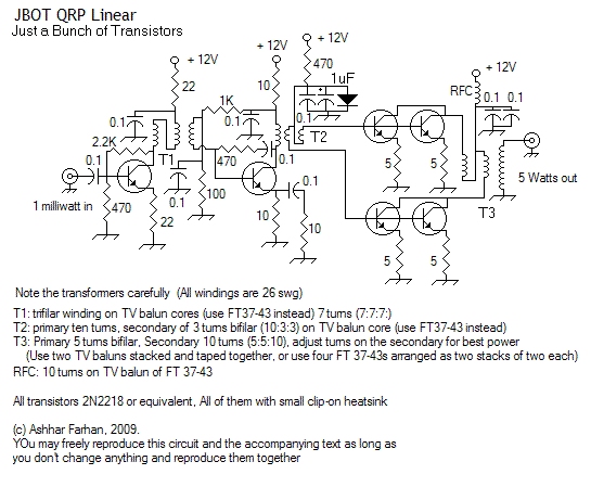
The first stage is set to a collector current of 50mA. This is on the higher side. It drives a trifilar transformer in the output.
The second stage is biased for almost 100 mA of current. This helps preserve the signal linearity. The bias for the base is routed through the secondary of the T1. The T2 transformer is a little tricky, the primary winding is simple 10 turns while the secondary winding consists of 3 bifilar turns around the core. The secondary is wired such that it becomes a center-tapped 3 + 3 turn winding.
The final stage uses four transistors in push-pull with two transistors on each side. Each transistor has a separate emitter degeneration resistor of 5 ohms. Each side is expected to push out 3 watts. This makes the output impedance of each side 25 ohms. The two sides in push-pull will add up their impedances and we will have 50 ohms across the primary winding of T3. The T3’s primary consists of 5 bifilar turns (5 + 5 = a total of 10 turns). Against this, the T3 a secondary winding is normal 10 turns.
Though the circuit is stable and works well throughout the HF spectrum (I haven’t measured it below 4MHz and above 28 MHz), be careful of operating it without load. The 2N2218s cannot handle more than 30 volts across them, so never operate without a proper load.
Construction:
For a change, nothing is critical in this power amp! The transformers need to be explained. Here goes,
T1: This is easy, it is a trifilar winding. If you imagine that the three wires of the transformer are A-B, C-D, and E-F. Then short B and C to make the center tap. Use A and D as the opposing ends of the primary and use D-E as the secondary.
T2: First wind three turns of twisted, bifilar wire as the secondary. Over this, wind ten turns as the primary. Short the two opposing ends of separate bifilar windings as the center tap and use the remaining, opposite ends of the secondary as the outputs that go to the output transistor bases.
T3: The output transformer is constructed out of two TV baluns stacked and taped together. Alternatively, the core can be made by first stacking two FT 37-43 and forming a cylinder, then two such cylinders are held parallel to each other and taped tightly. This forms a ‘double barrel’ through which the windings are made.
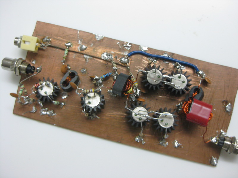
All transistors have small clip on heat sinks. Check the picture.
Tip: The 5 ohms resistor on each of the transistors should show a little more than half a volt across it, if it doesn’t you can assume it is blown.