A Simple Dual-band Transceiver

A dual-band transceiver with a crisp receiver and a clean SSB signal is described. It started its life as an investigation of the excellent S7C receiver described in EMRFD.
This transceiver was specifically designed to use components that are easily available in TV and Radio spares shops. The receiver sports an above average dynamic range, very clean signal and noiseless performance. Although the components are easily available, and every detail about making it is covered here, this is not a weekend project. The design is elaborate and invites improvisation.

We decided to pursue the following rules in designing this transceiver:

  • Use what is easily available. Very often, we find designs that look good but they use exotic parts like TUF-1 mixers that are simply impossible to get hold of in India and other countries. Instead, we have tried using those spares that are universally available.
  • Keep impedances and gain low: Often, we try coaxing maximum gain out of a stage making it difficult to duplicate and stabilize. We chose to take only modest gain out of each stage, using extensive feedback to make the circuit stable. Most of the interconnections between modules are for 50 ohms termination. In fact, the rig was a number of discrete board connected using RCA audio cables and sockets before we hooked it all up together to work.
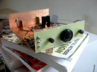
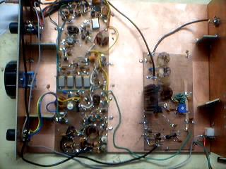
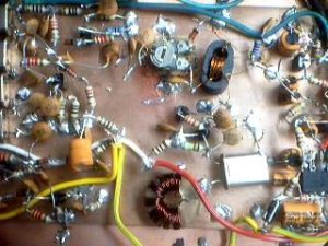
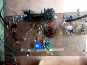
  • No PCB. We directly solder the components over a plain copper clad board (un-etched PCB). It is an excellent way to experiment, physically robust and has a quick and dirty appeal. You can usually solder up a whole circuit as you think it out in a few minutes. See the pictures.
  • Broadband. We wanted to be able to use broadband design where applicable. We have found that the television balun cores are an excellent and very cheap (about Rs. 2 per balun, that is 5 cents) way of making broadband transformers.
  • Modest cost. While we didn’t want to use very expensive components. We didn’t want to compromise the performance either. You will see that we have used 2N3866 exclusively. This was because we found that the BF195/BF194/2N2222 series transistors available in the market were consistently inferior in the HF range and performed below their stated specs. The 2N3866 is commonly used in cable TV equipment and has a good HF performance: both as a low noise small signal transistor as well as driver up to 1 watt level. 2N3866 is expensive (about Rs.20 each, but well worth the expense). It is used in a number of critical places.
  • Measure what you have built. We used a 12 volt 1.5A power supply, a frequency counter, a test oscillator (to measure the crystals and coils) and a high impedance voltmeter with an RF probe to test and measure the design. All these test equipment were homemade. The transmitter design did require a PC-based oscilloscope. It helped us identify the spurs and harmonics using the in-built FFT functionality. But now that the design is complete, just an RF probe and a 14MHz receiver are enough to align the rig.
  • Quality over quantity. A better signal is preferred to a bigger signal. This is a 6 watt design that will work off a simple 12V, 1.5A supply (using a single 7812).

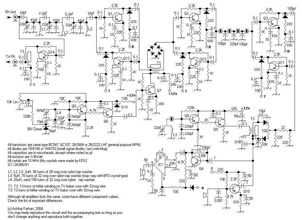
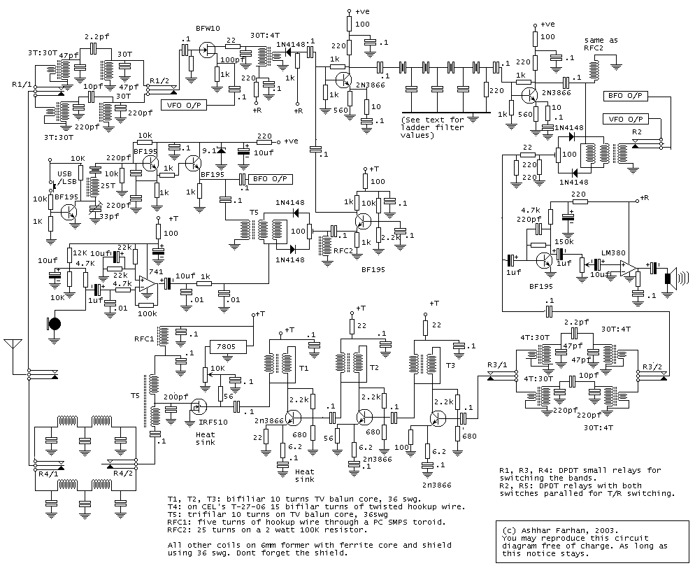
    The ladder crystal filter

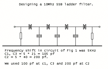
    A good filter is central to the crispness of a receiver and the quality of the transmitter. There are two types of crystal filters possible, the lattice filter and the ladder filter. The lattice filter requires ordering crystals with 1.5 KHz frequency difference between them. This was ruled out, also procuring readymade filters from BEL India and other sources was ruled out as it is too expensive to do that. Instead, a ladder filter was chosen. The ladder filter offers results as good if not better than a lattice filter. However, the design is crucially dependent upon internal parameters of the crystals used. It is not possible to suggest any generic values for the capacitors to be used in the ladder filter. Rather, a method to measure each of the crystals and calculate the capacitor values has been worked out. We present this here. This design procedure will work only for 10 MHz crystals. 10Mhz is the chosen IF of our filter as the crystals are easily available and it sits comfortably between 7 and 14 MHz amateur bands. We have followed the Butterworth design methodology given in the new ARRL book Experimental Methods in RF Design.

    The circuit centers around a four crystal ladder filter. Each lot of crystals from each manufacturer differs from the others. We will describe a way to experimentally calculate the values of the capacitors for the filter. You should probably buy 10 crystals and select 5 of them.

    For this purpose, we used a simple clever technique of measuring the motional parameters of the crystals. This technique has been developed by G3UUR. It works as follows:

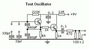
    Construct the test circuit of figure 1. This is a simple Hartley-style crystal oscillator. You will require access to either a frequency counter or a general coverage receiver (ask a neighborhood ham to allow you to bring over your crystals to his shack and test them for few minutes). Mark each crystal with a number and solder it into the circuit (don’t use a crystal socket). Connect the 9 volt battery and measure the frequency. If you are using a receiver, find out the frequency on which the crystal is absolutely zero. Note the frequencies with the 33 pf capacitor in series and shorted. You will have a pair of frequencies for each crystal. Select four crystals with pairs of frequencies that match within 50-40 Hz of each other. A fifth (for the carrier) oscillator crystal should be within 100 hz of the other four selected.

    Calculate the value of the capacitors of Fig.2 like this:
    1. Calculate the average frequency shift of the four chosen crystals as F (in KHz).
    2. C1 = 21 * F, C2 = 40 * F. Choose the nearest available fixed capacitor. If you can’t find a fixed capacitor within 10% of this value, then parallel two capacitors to achieve the capacitance.
    For instance, in the case of the first prototype, we measure an average of 5KHz of shift. Thus, the capacitors calculated were 107pf and 200pf. We used 100pf and two parallel 100pfs as a substitute for 200pf capacitors. These calculations are for 200 Ohms termination. For a complete discussion of this design method, you are referred to the excellent paper by Carver in the Communications Quarterly of 1993, Winter.

    Broad-band design without Toroids

    It was decided to use broad-band techniques where suitable and keep the circuit free of too many critically tuned circuits. We decided to investigate the TV baluns as cores for broadband transformers. The TV baluns are small ferrites as shown in the picture.


    Almost all the broadband transformers are bifilar. Two (the modulator and the transmit mixer cum product detector) are trifilarly wound. They are simple to produce.

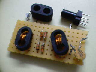
    (The small board holds a Double balanced diode mixer using the baluns, an unwound balun is shown next to it. the coil former in the picture is the one used throughout my projects).

    Making a bifilar transformer:

  • Take two lengths of 36 swg copper enameled wire.
  • Hold them together. Tie one end to a nail.
  • Twist the wires together so that they cleanly have about 8-10 turns per inch.
  • Check that the wires are evenly twisted (although there will be more twists towards the ends).
  • If the balun core is mounted on a PCB, cut it out with a cutter and remove all the original windings.
  • Pass the twisted pair through one hole to the other side, bend the wire back and pass it back through the other hole (like a U turn). This is one turn, like this, make similar 10 turns.
  • Cut out the remaining ends of the windings leaving about half an inch of the twisted pair on each end.
  • Scrap the enamel off to about quarter inch, and tin the leads.
  • Using a VOM at low ohms setting, identify the two separate windings of the twisted pair. If we call the two wires X and Y, each will have two ends A and B. This you will have four ends AX, BX, AY and BY. Short AX and BY together and use this as the center point of the transformer in the circuits. Use AY and BX as the two opposite ends of the transformers.Making a trifilar transformer is similar, except that you have to use three wires twisted together. Separate out the three wires as before, use the first two as described above, and the third winding as the secondary.

    IF sub-system

    The crystal filter and its associated IF circuitry is shared between the receiver and transmitter. Although the crystals are inexpensive enough to be able to afford separate filters for the transmitter and the receiver, we noted that each filter would have a different center frequency. This would make zero-tuning difficult for SSB operation. Therefore, it was decided to share the same crystal filter, carrier oscillator and the VFO between transmit and receive functions.

    The crystal filter requires 200 ohms impedance matching at both ends to provide the correct bandwidth and low ripple. A regular practice among hams is to strap a resistor of approximately the same value as the terminating filter impedance across the input and output ends of the filter. This is incorrect. This looks like a resistor that is paralleled with a reactive impedance of the rest of the circuitry attached to the filter. When the crystal filter is not properly terminated and sees reactive termination, ripple and ringing are introduced. This will spoil the crispness of the receiver and spoil your on-the-air quality.

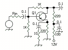
    The crystal filter is terminated on both sides by strong RC coupled amplifiers based on 2N3866. This is slightly unusual. The 2N3866 is used mostly as a VHF power amplifier. It has excellent low-noise characteristics, good gain and using it as a small signal device is now an established practice. The 2N3866 is an expensive transistor. It costs about Rs.20 in the open market. We think it is a good investment.

    Using RC coupled broadband amplifiers makes the IF system a no-tune affair. The output of the post-filter amplifier is coupled to a two diode mixer. The two-diode mixer uses a broadband bifilar wound transformer. It is next to impossible to get toroids in India. We have evaluated using TV baluns as substitutes for toroids. These baluns are available at most TV spare shops.

    Most designs we have studied couple the RF input to the diode detector through the transformer and inject the BFO at the center of the transformer. This is a wrong practice. The diode mixer requires a minimum of 5mW of energy from the transformer input to operate properly. There should be enough energy to switch on both the diodes. This means about 1.2 v peak voltage. The received signals are rarely this level. As a result, the product detector operates like a regular envelope detector and the diodes act as distortion devices to mix the BFO with the signal. The correct configuration is to inject the BFO across the transformer

    An unusual approach is taken here. The IF amplification gain is just enough to maintain good noise figure and recover the losses in the ladder filter. We measured almost 10 dB loss in the filter.

    The Receiver

    The receiver is minimal. By keeping the number of active devices low (3 devices between the antenna and the audio amplifier), very good fidelity is achieved. The circuit is kept at a low impedance and broadband everywhere except the front-end. This helps in stability.

    The front-end uses a low-noise FET. We have used a BFW11 (because the local component shop ran out of BFW10). They have slightly different characteristics. Almost any FET can be used if it is biased properly. The FET should be biased for exactly half the pinch-off voltage. Wes Hayward (W7ZOI) has described the proper way to bias a FET Mixer for proper operation.

  • Short gate and source and measure the current that flows through a 560 ohms resister connected to +12V through the drain. This gives the exact Idss.
  • Place a 10K resistor between the source and the ground. Keeping the gate grounded and the drain still connected through the 560 ohms resister, measure the voltage between the source and the ground. This gives you the pinch-off voltage.
  • The FET has to be biased such that the voltage on the source is exactly half the pinch-off voltage and there is half of Idss current flowing through the FET.Such a scheme assures you that the FET is driven between pinch-off and maximum drain by the VFO injected at the source. This gives the proper switching action for the mixer to operate as well as maximum gain. We measured the pinch-off voltage for BFW11s as 2.1 volts and Idss as 5mA. A standard 1K resistor at the source gives the proper bias.It should be noted here that we first tried a double balanced diode ring mixer at the front-end. It has a number of spurious responses that literally made it impossible to use the receiver. We tried to properly terminate the diode ring mixer by inserting attenuators between the mixer and the Ladder filter’s pre-amp. It didn’t cure the problem. When we changed to the FET mixer, the noise figure improved, the receiver’s dynamic range, while unmeasured, was never found lacking in the last one month of extensive usage at VU2PEP.The output of the IF amplifier is detected in a balanced detector using just two diodes. Here gain, we break a common myth. You will see most of the HF receivers employing a two diode balanced detector with the BFO fed to the center tap and the incoming signal applied through the primary winding of the detector transformer. This is wrong. The signal applied through the primary winding should strong enough to switch the diodes on and off (requiring about 0.6 across each diode, that is, 1.2 volts across the winding). This roughly translates to about 5 mW power. The diodes switch the low level signal coupled at the center-tap of the coil to the detector output. Therefore, in our design we have applied the local oscillator through the primary of the transformer and the incoming signal from the IF stage to the center tap.

    There is a 100 ohms preset used to null the local oscillator from appearing at the output. This is of importance during transmit where the balanced detector also doubles up as the transmitting mixer.

    An audio pre-amplifier follows the detector. The capacitor of 220 pf between the base and the collector ensures that the hiss is kept down. The audio amplifier used is an LM380. Almost any audio amplifier can be used. We have tried everything from the PC’s ampli-speakers to a Sony amplifier to a TBA810 amplifier. We would recommend using a high fidelity, low cost amplifier like the TBA810 if you plan using a speaker. If most of your work is with headphones (to save your companion from the late night QRM), we recommend the LM386.
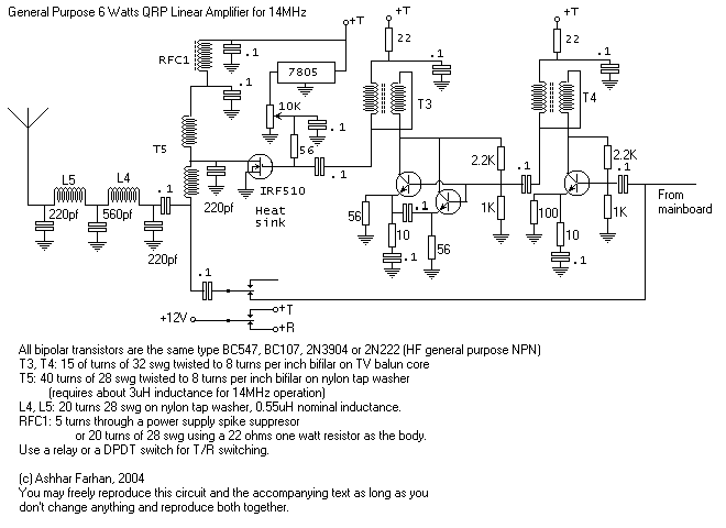
    The Transmitter

    The transmitter starts with the modulator using a 741. There is a three resistor network that biases the electret microphones. We use a Phillips “walkman” style headphone with built-in microphone for our work. The electret microphone requires a bias that provides 5V as given by the circuit.

    The balanced modulator also had two 22pf trimming capacitors for nulling the carrier. They were later found unnecessary (as long as both the diodes are purchased from the same roll) and removed. If you do find balance a bother, feel free to add a 22 pf trimmer to one side and a 10 pf fixed to the other side as indicated in the schematic.

    The output of the balanced modulator is routed to the common IF amplifier through a buffer amplifier using a BF195. This serves to keep the carrier leak from the modulator out of the IF string during the reception mode.

    The balanced detector of the receiver also doubles up as a mixer during transmit. It is important to balance out the VFO energy at the output by setting the 100 ohms trimmer properly. We noticed a 50mW residual out-of-band output from the transmitter when the VFO is unbalanced.
    The power chain is an interesting broad-band amplifier. You can use this in virtually any transmitter of up to 7 watts (and higher with more than 12 volts supply to the final stage). Three stages of broadband amplifiers feed an IRF510 PA. It is an interesting twist that the driver 2N3866 transistors cost more than the IRF510! The IRF510 should be biased for 80mA of standing current during transmit with the microphone disconnected (no modulation) and carrier nulled by the trimpot of the balanced modulator.

    Construction

    We heavily recommend constructing over pieces of un-etched PCBs. They are cheaply available everywhere. See the pictures as a guide to component layout. We recommend the following rules:

  • Keep your leads short. Short connections are more important than components that are at right angles to each other. What might look neat to you might look unstable to the RF design.
  • Keep the outputs and inputs isolated from each other. We have taken care to keep the high impedance points down to a minimum. But still, maintain design hygiene.
  • Make one module at a time, test it completely, then move to the next one.Construct the transceiver in the following steps:
  • Make the VFO. Check the RF output using an RF probe. Check the stability on a regular receiver or a frequency counter. With the tuning capacitor fully closed (the plates inside each other), set the trimmer so that the VF0 frequency is exactly 3.9995 MHz (keep 5 KHz margin at the band end)
  • Make the BFO. Check the output on the RF probe.
  • Calculate the ladder filter values and make the IF strip along with the audio preamplifier.
  • Connect the BFO, VFO, IF strip and an external audio amplifier together. When you power on and attach a piece of 2-3 meter long wire to the input of the IF amplifier you should be able to hear the atmospheric noise. Tune the BFO coil by fully screwing the slug in and then slowly tuning it out until the IF noise sounds right (not too shrill and not too muffled).
  • Wire up the receiver mixer, connect the VFO. Peak the mixer output and the RF input coils for maximum output. Then tune to a weak signal on the band and tune for the best signal. Be careful to tune for best quality of signal and not for maximum loudness.Take a break, spend a day or two listening to the band with your receiver. Nothing is more enjoyable than using a crisp receiver that you have homebrewed.
  • Wire up the modulator. If you have an oscilloscope, you can check the modulation. The modulated output will be too low for you to be able to measure on the RF probe.
  • Wire up the linear chain. DON’T solder the IRF510 yet.
  • Put the transceiver in transmit mode. Whistle into the microphone and peak the transmit mixer output coils for about 6 volts peak RF voltage on the probe at the 56 ohms resistor where the gate of the IRF510 would be.
  • Solder in the IRF510. ATTACH A DUMMY LOAD. We used four 220 ohms two watts resistors paralleled together.
  • Keep the bias trimmer totally down towards zero. Attach VOM in series with point X in the power amplifier. Apply power in transmit mode and slow increase the bias until you have 80mA flowing through the IRF510.
  • Connect the RF probe across the dummy load.
  • As you whistle, You should get about 20-24volts of peak RF on the probe. When you pull out the microphone from the jack, the RF output should drop to complete zero.What if your transmitter is unstable?
    • Don’t curse your fate. All transmitters start out as unstable beasts. Relax.
    • Start disconnecting power from the stages starting from final IRF510 and working backwards. When you have located the unstable stage, there are a number of things you can do to fix it.
    • Try increasing the value of the 10 ohms resistor used in the emitter degeneration OR
    • Strap a resistor of about 1K across the output transformer of the unstable stage to ‘load’ it.
    • Move the linear amplifier away from the rest of the circuitry.
    • Redo the board. This time spread the stages out. We guess that the linear chain should occupy about 6 inches of space, all laid out in one line.

    Substitutions

    The BF195 transistors can be substituted with any other HF transistor like 2N2222 etc. The 2N3866s are best not subsituted. The circuit works with slight increase in the noise figure if BF195 or equivalents are used in place of 2N3866s in the IF stages. The output power on the transmitter absolutely needs the 2N3866s. Subsituting them with other switching transistors didnt give good performance.

    The IRF510 should not be subsituted with any other transistor. The other IRFs, though rated higher, have higher input capacitance which makes them a bad choice for 14MHz operation.

    The LM380/LM386 can be subsituted with almost any other audio amplifier. Our first amplifier were Cambridge SoundWorks Sound System. If you turn down the bass, they are an excellent system for the shack. We have tried a TBA180, an LM386, an LM380 and even a glow-bug guitar amp. Feel free to experiment.

    Final Notes

    The first contact we made using this rig was DF6PW. He reported us 57. Within the first evening we had worked four continents. The rig was regularly used at VU2PEP. People are often surprised at how the transmitter quality is  “just like a commercial rig”. Many refused to believe that it is a seven watt rig.

BITX – An easy to build 6 watts SSB transceiver for 14MHz


BITX is an easily assembled transceiver for the beginner with very clean performance.
Using ordinary electronic components and improvising where specific components like toroids are not available, It has a minimum number of coils to be wound.
All alignment is non-critical and easily achieved even without sophisticated equipment. The entire instructions to assemble the rig are given here along with relevant theory.

The Indian hams have often been handicapped by a lack of low cost equipment to get them on air. A mono-band, bidirectional design using ordinary NPN transistors was developed to cater to this demand. The design can be adapted to any particular ham band by changing the RF section coils and capacitors and the VFO frequency.

BITX evolved over one year from the excellent S7C receiver described in the new ARRL book Experimental Methods in RF Design (an ARRLpublication) into a bi-directional transceiver. Several hams across the globe contributed to its design. A series of emails were exchanged with OM Wes Hayward (W7ZOI) during the evolution of this design. His contributions have been invaluable. He urged me to strive for higher performance from the simple design. The resultant rig has sensitive receiver capable of strong signal handling, a stable and clean transmitter capable of enough power to make contacts across the World.

All the parts used in BITX are ordinary electronic spares components. Instead of expensive and hard-to-get toroids, we have used ordinary tap washers. Broad-band transformers have used TV balun cores.

For those who don’t read long articles …

There are a couple of things you should know before you start assembling the circuit:

  • The same amplifier block is used throughout. But the emiiter resistors vary in some of the places. Double check the values. If you swap values, the circuit won’t stop working. It will work terribly. That might be a little difficult to diagnose in the end. Check the emitter values and the resistors that go between the base and collector.
  • The receiving IF amplifier between the filter and the product detector is coupled to the product detector using a 100pf (not 0.1uf).
  • The crystal filter worked for me, I used crystals from the local market marked as KDS. These are the cheapest and they work with the capacitor values given in the filter. Your crystals might require a different set of capacitors. Try the values given here, if you find the bandwidth too narrow, decrease the capacitances, if you find it too open then increase the capacitances.
  • The microphone is directly coupled to the amplifier as my headset microphone needs 5V bias. If your microphone works without bias, then insert a 1uf in series with the microphone.
  • The pictures show my prototype on two boards. Don’t do that, split up the VFO into a separate box.
  • The pre-driver is built onto the main board. The driver and the PA are on a separate board. Keep the same layout to keep the PA stable.
  • There is a 50uf on the power line soldered near the BFO, don’t forget it. It cleans up the audio noise which would otherwise get into the receiver.
  • On the PCB, there are jumpers between T lines and R lines across the ladder filter. There is a jumper from the BFO supply to the VFO supply.

Development Notes

Almost all modes of radio communications share a natural principle that the receivers and transmitters operate using the same line-up of circuit blocks except that the signal direction is reversed. The CW direct conversion transceiver is the simplest illustration of this principle. A more complex example is the bidirectional SSB transceiver.

Bi-directional SSB transceivers have been quite common in amateur literature. A transceiver was described in the ARRL SSB Handbook using bipolar transistors. W7UDM’s design of bidirectional amplifier (as the basis of bidirectional transceiver) is referred to by Hayward and DeMaw in their book Solid State Design. The bidirectional circuitry is often complex and not approachable by the experimenter with modest capability (like me).

The broad band bi-directional amplifier

My current interest in bidirectional transceivers arose after looking at an RC coupled bidirectional amplifier in the book Experimental Methods in RF Design (p. 6.61). An easily analyzed circuit that was simple and robust was required. It began its life as an ordinary broad-band amplifier:

Figure 1

In any bipolar transistor, the current flowing from the collector to emitter is a multiple of the current flowing from the base to the emitter. Thus, if there is a small change in the current flowing into the base, there is a bigger change in the current flowing into the collector. What follows is a highly simplified explanation of working of the above amplifier.

In the above circuit, imagine that a small RF signal is applied through Rin to the base of Q1. Also imagine that the Rf voltage is swinging up. The transistor will accordingly amplify and increase collector current causing more current to flow through the Rl (220 ohms) collector load. This will in turn drop the voltage at the collector. The drop in voltage across the collector will also result in a drop at the base (base voltage is a fraction of the collector voltage due to the way the base is biased). This circuit will finally find balance when the increase in base current flowing from Rin is balanced by the decrease in base current due to the voltage drop across Rl. In effect the RF current entering from Rin flows out through the feedback resistance (Rf). The impedance seen at the base is effectively very low and the signal source will see an approximate input impedance of Rin.

Thus, Vin/Rin = Vout/Rf (Eq.1)

Another factor to consider is that that emitter is not at ground. At radio frequencies, it looks like there is a 10 ohms resistor between the emitter and the ground. Thus, when the base voltage swings, the emitter will follow it. The AC voltage variations across the Re (10 ohms) will be more or less the same as that across the base. The current flowing into the emitter will mostly consist of collector current (and very little base current). Thus, if the emitter current almost equals collector current,

Ie = Vin / Re = Vout / Rl (Eq. 2)

We can combine these two equations to arrive at:

Vout / Vin = Rf / Rin = Rl / Re. (Eq. 3)

This is an important equation. It means several things. Especially if you just consider this part:

Rf / Rin = Rl / Re. (Eq 4)

Let’s look at some interesting things:

  1. The voltage gain, and the input and output impedances are all related to resistor values and do not depend upon individual transistor characteristics. We only assume that the transistor gain is sufficiently high throughout the frequencies of our interest. The precise value of the transistor characteristics will only limit the upper frequency of usable bandwidth of such an amplifier. This is a useful property and it means that we can substitute one transistor for another.
  2. The power gain is not a function of a particular transistor type. We use much lower gain than possible if the transistor was running flat out. But the gain is controlled at all frequencies for this amplifier. This means that this amplifier will be unconditionally stable (it wont exhibit unusual gain at difference frequencies).
  3. You can restate the eq 3 as Rf * Re = Rl * Rin . That would mean that for a given fixed value of Rf and Re, the output impedance and input impedances are interdependent. Increasing one decreases the other and vice versa! For instance, in figure 1, Rf = 1000, Re = 10, if we have Rin of 50 ohms, the output impedance will be (1000 * 10)/50 = 200 ohms. Conversely, if we have an Rin of 200 ohms, the output impedance will be 50 ohms!

In order to make bidirectional amplifiers, we strap two such amplifiers together, back to back. By applying power to either of amplifiers, we can control the direction of amplification. This is the topology used in the signal chain of this transceiver. The diodes in the collectors prevent the switched-off transistor’s collector resistor (220 ohms) from loading the input of the other transistor. A close look will reveal that the AC feedback resistance consists of two 2.2K resistors in parallel, bringing the effective feedback resistance to 1.1K. Thus, the above analysis holds true for all the three stages of bidirectional amplification.

Diode mixers

The diode mixers are inherently broadband and bidirectional in nature. This is good and bad. It is good because the design is non-critical and putting 8 turns or 20 turns on the mixer transformer will not make much of a difference to the performance except at the edges of the entire spectrum of operation.

The badness is a little tougher to explain. Imagine that the output of a hypothetical mixer is being fed to the next stage that is not properly tuned to the output frequency. In such a case, the output of the mixer cannot be transferred to the next stage and it remains in the mixer. Ordinarily, if the mixer was a FET or a bipolar device, it usually just heats up the output coils. In case of diode ring mixers, you should remember that these devices are capable of taking input and outputs from any port (and these inputs and outputs can be from a large piece of HF spectrum), hence the mixer output at non-IF frequencies stays back in the mixer and mixes up once more creating a terrible mess in terms of generating whistles, weird signals and distorting the original signal by stamping all over it.

A simple LC band pass filter that immediately follows the diode ring mixer will do a good job only at the frequencies it is tuned to. At other frequencies, it will offer reactive impedance that can cause the above mentioned problems. It is requirement that the diode mixer’s inputs and outputs see the required 50 ohms termination at all the frequencies. In other words, they require proper broadband termination. Using broad-band amplifiers is a good and modest way of ensuring that. A diplexer and a hybrid coupling network is a better way, but it would be too complex for this design.

Circuit Description

Although simple, every effort was made to coax as much performance as was possible given the limitations of keeping the circuit simple and affordable.

The Receiver

The RF front-end uses a triple band-pass filter for strong image and IF rejection. The three poles of filtering are quite adequate and the out-of-band response of the receiver is only limited by external shielding and stray pickups.

An RF amplifier follows the RF band pass filter (Q1) biased for modest current. More current would have required a costlier transistor. There is 8mAs through the RF amplifier and the post-mix amplifiers to keep the signal handling capacity of the circuit above average. The Post-mix amplifier (Q2) does the job of keeping the crystal filter as well as the diode mixer properly terminated. The crispness of the receiver is more due to this stage than anything else. An improper post-mix amplifier easily degrades the crystal filter’s shape and introduces spurious signals and whistles from the diode mixer. Note that the mixer is singly balanced to null out the VFO component and not the RF port and in the absence of proper pre-selection, 10MHz signals can easily break into the IF strip.

The VFO is fed via a broad-band amplifier into the singly balanced mixer. We used the simplest VFO possible with a two-knob tuning mechanism. It works really well and for those (like me) used to quick tuning, it offers best of both worlds, slow tuning through the varactor and fast tuning through the capacitor without any slow motion drive. Getting a slow motion drive is an increasingly difficult problem and this is an electrical substitute for slow motion drives.

A word about the VFO: depending upon component availability, skills and preferences, everybody has a favourite VFO circuit. Feel free to use what you have. Just keep the output of the collector of Q7 to less than 1.5 volts (it will appear clipped on the oscilloscope trace, that is okay). For 20 Meters operation, you will need a VFO that covers 4 to 4.4MHz. The given VFO has low noise though it does drift a little, but I have had no problems with ordinary QSOs. After 10 minutes of warm up, the drift is not noticeable, even on PSK31 QSOs.

A Hartley oscillator using a FET like BFW10 or U310 would work much better. You can substitute this VFO with any other design that you might want to use. If you are using the PCB layout, then skip the VFO on board if you want to use a different VFO and build it externally in a separate box.

The simple IF amplifier has a fixed gain. Earlier it was noted that IF amp was contributing noise at audio frequencies. It was later traced to noise from the power supply and placing a 50uf on the transceiver power line has cured it. The IF amplifier has a 100pf output coupling to provide roll-off at audio frequencies.

The BFO is a plain RC coupled crystal oscillator with an emitter follower. The emitter follower has been biased to 6V to prevent limiting.

The detector also doubles up as the modulator during transmit mode; hence it is properly terminated with an attenuator pad. It has no impact on the overall noise figure as there is enough gain before the detector. The audio pre-amplifier is a single stage audio amplifier. The 220pf capacitor across the base and collector provides for low frequency response.

The receiver does not have an AGC. This is not a major short-coming. Manual gain control allows you to control the noise floor of the receiver and I personally find it very useful when searching for weak signals or turning it down to enjoy the local ragchew.

Transmitter

The microphone amplifier is DC coupled to the microphone. This was done to steal some DC bias that is required when using a Personal Computer type of headset. If your microphone does not require any bias, then insert a 1uF in series with the microphone. The microphone amplifier is a simple single stage audio amplifier. It does not have any band pass shaping components as the SSB filter ahead will take care of it all. One 0.001uf at the microphone input and another at the modulator output provide bypass for any stray RF pickup.

The two diode balanced modulator uses resistive as well as reactive balancing. A fixed 10pf on one side of the modulator is balanced precisely by a variable 22pf on the other side. A 100 ohms mini preset allows for resistive carrier balance. The attenuator pad at the output was found necessary to properly terminate the diode modulator and keep the carrier leakage around the IF amplifier to a minimum. While this may seem excessive, it produces a clean DSB with carrier nearly 50db down with careful adjustments on the oscilloscope.

Rest of the transmission circuitry is exactly the same as the receiver. There is an extra stage of amplification (Q14) to boost the very low level 14MHz SSB signal from output of the microphone tip to driver input level.

The output amplifier boosts the SSB signal to 300mV level, enough to directly drive a driver stage.

The Power Chain

A simple power chain consisting of a low-cost medium power NPN transistor (2N2218) driving an IRF510 for 6 watts of power at 14MHz. The output of IRF510 uses a tap washer as an output transformer. The output transformer has 40 turns of bifilar winding; these can lead to enough stray capacitance to affect proper performance as a transformer. The half-wave filter that follows the transformer absorbs these capacitances as a part of the matching network.

I used this power chain because it works for me and delivers 6 watts on 14MHz. I don’t use more power because I neither require more nor do I have a power supply that can source more. If you need more power, there are a number of things that you can do, you can simply increase the supply voltage on the IRF510 up to 30 volts and extract nearly 15 watts of power from the same configuration. At 30 volts, the drain output will be at 30 ohms impedance and the pi-network will have to be designed to directly match the drain to a 50 ohms antenna load. Alternatively, you could try two IRF510s in push-pull. These are variations that you can play with. A word of warning though, The RF energy at these levels can give you a serious RF burn. RF burns can be more painful than fire or steam burns. QRP is not only fun, it is also safe.

Construction

I would highly recommend that you construct it over a plain copper clad board by soldering the grounded end of the components to the copper and the other ends of components to each other. Look at the pictures to see how it has been done. If you don’t know about this method of assembling RF circuitry, then you should read about it, there are quite a few write ups on the Internet about this method of RF experimentation. It does not require any PCB, it is quite robust and very stable.

Assembling the PCB (The text on PCB is only for archival purpose, there is PCB available now)

For those who feel intimidated by this Ugly method, I have designed a PCB. The PCB layout (component side) is provided with this article. It is a single sided PCB with wide tracks that can be easily made in the home lab. I am making a run of these PCBs but shipping them abroad (outside India) maybe a problem. Drop a mail to me if you are planning to make some PCBs, I can put your contact information on the website. There are no copyrights over either the PCB, the circuit or even this article, feel free to copy and distribute.

The PCB is laid out in a long line.It is 8-1/2 inch long and 2-1/2 inch wide. The circuit board is big for the circuit that goes onto it. This was done so that the board is non-critical and it works well. All the bidirectional amplifiers are similarly laid out.

When you get your PCBs, inspect them thoroughly, preferable in the Sun. Check for small cracks in the tracks. Check for tracks that might be touching each other or touching the ground plane. The PCB layout was done to minimize this, but check it anyway. Especially check for the tracks that run diagonally to the base of each transistor in the bidirectional circuitry. These are laid out very closely and they are candidates for shorting.

Almost all assembly instructions ask you to solder the transistors in the end. I would highly recommend that you solder the transistors and the diodes first. You are most alert when you start a project and if you place the transistors correctly, the rest of the circuit can be soldered around it. Be very careful about the orientation of each transistor. The microphone amplifier transistor (Q10) faces in a direction opposite to the rest of the transistors and the transistor pairs in bidirectional amplifiers face each other. The diodes have a ring to indicate which way their arrow is pointing.

After the transistors are soldered, finish the BFO. If you are assembling this for 14MHz and above, the BFO will need a coil in series with the crystal (USB mode), if you are need LSB operation, you will need a trimmer instead (see the schematic). Apply power to the BFO and you should be able to hear it on your Short wave broadcast radio around 31 meter band. It will sound like a silent radio station. It should be quite strong. Switching the BFO power supply on and off will help you identify your BFO signal on the radio. If you have an RF probe, or an oscilloscope, you should be able to see the oscillations. Expect RF of 2 volts or more.

Next, assemble the VFO. Winding 150 turns of the VFO coil is one of the most tedious jobs while assembling this rig. It has to be done, so just dig in and do it. You don’t have to attach the 365 pf tuning capacitor yet. Check the oscillations on a receiver or a frequency counter. You may have to decrease the number of turns. Without the 365 pf, the 22pf trimmer should be able to set the VFO to 4.3MHz or so. If the VFO is oscillating at a lower frequency, then remove some turns from the coil. If the VFO is at a higher frequency, add 22pf in across the 22pf trimmer (if you are using the PCB, solder in from the foil side). You will require a wire jumper to carry power supply between the VFO and the BFO.
They are the only stages that remain switched on during both transmit and receive.

Assemble the audio pre-amplifier and the audio power amplifier and attach the volume control. When power is applied to the audio stages, touching a finger to the base of Q4 should produce static in the speaker to move even the most die-hard trash metal rockers.

Next, assemble all the three bi-directional stages! This involves lot of soldering. But all the six stages are exactly the same. Finish one stage at a time. The capacitors are symmetrically laid out and all of them are 0.1uF with one exception (100pf at the output of Q3). Remember that the emitter bias resistors are 100 ohms, 220 ohms or 470 ohms. If you mix up the values, the rig will still work but it will under perform in the presence of strong signals and the transmission will be splattered. There are jumpers for T and R line across the crystal filter. Solder them up and power on the R line and then the T line alternatively. The emitters of bidirectional stages should show 2 volts approximately and the collectors should show around 8 volts and the switched-off transistor should show zero voltage on all the three leads.

For the moment of truth, solder the three coils, trimmers and capacitors of the RF filter, attach an antenna and switch it on! Check that the stages are working starting from audio end. If you touch the volume control’s centre pin, you should hear AC hum and static. If you touch the base of Q4, there should be a pretty loud static. Take a lead from your VOM and touch Q3, you should get very loud static, probably mixed with local AM broadcast. Touch the base of Q2 with the test lead and you should get lesser static as the filter allows only 3 KHz of 10MHz through.

Finally, connect the antenna properly at the input of the RF band-pass filter and peak up the three trimmers for maximum atmospheric noise. Attach the 365 pf and start tuning around the band, peak the RF front-end on a strong signal and then tune in a weaker signal and peak for maximum clarity (not maximum sound).

An important note: Be sure that you have connected a proper 50 ohms antenna load. The RF filter performs correctly only at 50 ohms. If you use a long wire to do the initial testing, you will have to touch up the trimmers again for the proper antenna.

Take a break, spend the evening listening to your new homebrew. If the CW signals tune to dead beat and rise on the other side again, your BFO has to move its frequency. For USB, add more turns to the coil to the BFO coil, for LSB, tweak the trimmer. You should have a perfect single signal reception. If you tune past the dead-beat of a CW signal, the signal should drop out completely.

Assembling the microphone amplifier (Q10) and the output amplifier (Q14) will complete the exciter portion of the transceiver. To put the transceiver in transmit mode, ground the R line and apply 12V on the T line. Attach the output of Q14 to an oscilloscope but don’t attach the microphone yet. Null the carrier with the 100 ohms preset and the 22pf trimmer. Each affects the other so you might have to go back and forth between the two controls.

Now plug-in the microphone and speak into it. You should be able to see clean SSB of between 200 and 300 mV on the scope at the output of Q14. Instead of the oscilloscope you can use another 14MHz receiver to test your transmission quality. Switch off the AGC of the other receiver while setting the carrier null. A soft whistle (if you can manage) into the microphone is should result in a full carrier at the output.

Next, assemble the power chain. At this point, you will need a suitable chassis to house your project. Any metal box will do. If you don’t have any, you can solder pieces of copper clad together (like I did) and make a U shaped chassis. Keeping the VFO in open air makes it drift a bit. A closed box is really very useful.

A big cookie (or chocolate) box of tin is really ideal. With a hand drill, you can easily make holes to fit the two PCBs inside it. Tin is easily soldered on. Use the biggest knob you can find for the main tuning. The plastic broadcast capacitors usually have a very short stub that cannot take a big knob. It takes on a small plastic drum that is held onto the capacitor spindle with a retaining screw. Clip on the drum onto the tuning capacitor, tighten the retaining screw well and with epoxy glue, stick a big knob over the drum. This will make your main tuning mechanism.

I use a simple double pole triple throw switch for Transmit/Receive switch-over. If you prefer PTT operation, you can easily substitute the switch for a relay. Be sure to solder a reverse biased diode across the relay coil to prevent reverse voltage from entering into the transceiver power line.

Use shielded cable for all the connections between the power amplifier and the main board.

Tune-up and Operation

Set the VFO to correctly cover 4.0 to 4.4MHz. If you can, take your rig over to a ham friend’s shack, you can monitor your VFO on his rig at the edge of 80 meters band at 4.0MHz. Set the trimmer so that you can hear the VFO when the friend’s receiver is tuned to 4.0MHz and your tuning capacitor is fully closed (as much as it will go anti-clockwise). After this, connect the antenna and peak the RF coils for maximum noise in the speaker. If you can tune it to a weak signal, then peak the RF coils for best reception.

You might find that although you are able to tune in CW stations, you are unable to hear the SSB stations properly. This indicates that your BFO is not properly set. We will take that up next.

On amateur bands above 10MHz, SSB is transmitted on upper sideband and on bands below 10 MHz, it is transmitted on lower sideband. To tune a upper side-band signal, your BFO has to be at the lower edge of the crystal pass-band. You will require either the inductor (for USB) or the capacitor (for LSB) in series with the BFO crystal. If your BFO is set to proper frequency then the signals will tune in and as you continue tuning across the signal, they will drop in pitch and disappear. If the signals appear muffled, then the BFO is set in the crystal filter’s center, add more turns to the coil (USB), or tweak the trimmer (LSB). If the signals appear shrill and you are unable to zero-beat them, then the BFO is too far away from the filter’s frequency – Decrease the coil’s turns (for USB) or tweak the trimmer (LSB).

The transmitter tune-up essentially involves setting the carrier null. It is best to tune up the transmitter on a dummy load. I use 8 220 ohms, 2 watts resistors in parallel as my dummy load. It is worth the few bucks to have a proper dummy load. Attach the dummy load on the transmitter, and attach an RF probe to the dummy load (or an oscilloscope). As you speak, you should get 20 volts or more peak voltage on the dummy load when you whistle or just go “haaaaallow”. On another receiver in the same room, connect a short piece of wire as an antenna and monitor your own signal. You will probably be able to hear your own carrier as well. Null it by tweaking the 100 ohms preset and the 22pf balance trimmer. They both interact, so you might have to go back and forth between the two controls.

A word of caution, the diode mixers are prone to generating odd harmonics. The third harmonic of 4 MHz is at 12MHz. So, if you simply peak the coils for maximum output on transmit, you might wrongly peak the RF front-end to 12 MHz (I did that). The RF band-pass filter is best tuned in receive mode over a weak signal at 14.150MHz or so and left at that.

Conclusion

There might be a kit (components and the PCB in a bag) soon. I personally don’t have the time to put kits together. If somebody is interested in doing so, just go ahead and do it. The design is free, you don’t need to ask my or anybody else’s permission. If you can drop me a line, I will list you as a kit supplier on my site.

This is also the first time I have put out a PCB design for my rig. The purpose is to address the need among Indian hams in particular for an SSB rig that is easily and cheaply built. My original aim was to keep the price under Rs. 1000. The current design brings the cost to well under Rs.300 (less than 7 dollars).


Pictures


The top view of the transceiver
The big board has the entire exciter. The smaller board on the right is the linear


The IF and audio section
The present was soldered onto a small piece of vero-board (copper side) and the vero-board was in turn soldered onto the ground plane with small pieces of wire.


The RF front-end
shows only two coils in the RF filter, the third was added later. The upper coil is the VFO. The mixer transformer is seen on the lower right part of the picture.


The Power chain
The IRF510’s heat sink is soldered onto the ground plane. Use a mica washer to isolate the IRF510 from the heat sink.


The PCB layouts (No longer available)

The main board is 8.5 inches by 3 inches. The power amplifier board is 4 inches by 2.5 inches.

Download the PCBs here

Note: The PCBs are in GIF format. They are also in word doc format so that they print at correct size.
If you are getting the PCBs made somewhere, be sure to tell them the exact dimensions of both the boards.